These pages are meant mainly for engineering students studying in second year( Mumbai university only). If you are from some other university then confirm with your professors whether these formulae/methods are valid for your university.
mod(Av) = (hfe * RL')/(hie + (ðh * Rc) )
Where ðh = ((hie * hoe) - (hfe * hre)) [Get hfe, hre, hie,hoe from data sheet]
[if min voltage gain is specified, use hfe min. If some specific voltagegain is specified, use hfe typ]
Calculate RL' & Rc
Select higher std value for Rc to increase voltage gain [if min voltage
gain is specified or nothing is specified. If max voltage gain
is specified use lower std value. If some specific voltage gain is
specified, use nearest std val]
Vceq = Vcc/2
[If Vcc not given]
Vceq = 1.5(Vo peak + Vce sat)
Ic peak = Vo peak / RL'
Icq = Ic peak + Ic min
[Unless specified] Assume Ic min = 0 or 0.005 mA
[If Vcc given]
Vre = 10% of Vcc
Re = Vre/Icq
Select lower std value of Re so that voltage drop across Re is less
which increases the voltage swing of o/p
Assume higher std val [typically 9,12,15,18]
s = (1 + hfe max)/(1 + ((hfe max * Re )/(Rb + Re))
Find Rb[Do not standardise]
Vr2 = Vbe + Vre
Vr1 = Vcc - Vr2
Assume Vbe = 0.6V [for Si, 0.3 for Ge if not specified]
R1/R2 = Vr1/Vr2 .............(A)
[Get R1 in terms of R2 & substitute in Rb]
Rb = R1 parallel R2 = (R1 * R2)/(R1 + R2)
Find R2
Select lower standard value to make circuit indepent of beta
Substitute in (A) to find R1
Select higher standard value so that circuit draws minimum current
from supply
[If Rs[Source resistance] is not specified assume Rs = 0]
Xcb = Rs +((Rb) parallel (hie))
Cb = 1/(2 * pi * FL * Xcb)
Xcc = Rc + RL [If RL[load resistance] is not specified thenassume amplifier is connected to a similar next stage. Hence RL = (Rb)parallel (hie)]
Cc = 1/(2 * pi * FL * Xcc)
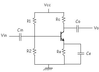
[Draw the figure with designed values. Do all this in 30 minutes (1.8 min per mark)]
Zin = (Rb) parallel (hie)