These pages are meant mainly for engineering
students studying in second year( Mumbai university only). If you are from
some other university then confirm with your professors whether these formulae/methods
are valid for your university.
Home
BJT
single stage amplifier designing
FET single stage amplifier designing
BJT multistage amplifier designing
Power amplifier designing
Solved problems
Design of single stage
JFET amplifier
1: Design for device parameter
variations
2: Design for midpoint biasing
3: Design for Zero thermal drift
4: Graphical methord
[Do not write text included in square bracket ]
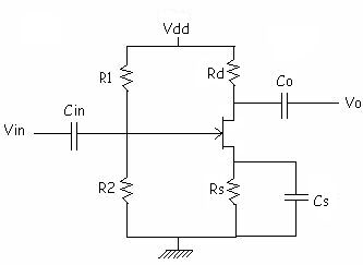
Type 1:Design against
device parameter variations
Step1: Selection of biasing circuit
We select voltage divider bias circuit as it provides stable
quiescent point against device parameter variations
[Draw the figure]
Step 2:Selection of Idq
Given Id min & Id max
Idq = (Idmin + Id max)/2
Step 3: Selection of Vgsq
Id = Idss * sqr(1- (Vgs/Vp))
Vgs = Vp * (1 - sqrt(Id/Idss))
Calculate Vgs max by substituting Vp max, Id max & Idss max
inVgs
Similarly calculate Vgs min
Vgsq = (Vgs max + Vgs min)/2
Step 4: Selection of Rs
Rs = (mod(Vgs max) - mod(Vgs min))/(Idq max - Idq min)
Step 5: Selection of Rd
gm = gmo(1 - (Vgs/Vp typ))
Gain of JFET amplifier, mod(Av) = gm * RL'
If RL is given
RL' = (rd) parallel (Rd) parallel (RL)
If RL is not given
assume RL = infinity
RL' = (rd) parallel (Rd)
Calculate Rd from above
[If required gain(Av) is greater than a specified value, select higher
std value]
[If required gain(Av) is equal to a specified value, select nearest
standard value]
Step 6: Selection of Vdsq
Case 1: Vo is given & Vdd is not given
Providing 15% margin we get
Vdsq = 1.15 * (mod(Vp typ) + Vo peak)
Case 2: Vo is not given & Vdd is given
Vdsq = (mod(Vp typ) + Vdd)/2
Case3: Vo is not given & Vdd is not given
Assume Vo = 1.5 V
Vdsq = 1.15 * (mod(Vp typ) + Vo peak)
Step 7: Selection of Vdd
Vdd = Idq * (Rd + Rs) + Vdsq
Select higher std value
Step 8: Selection of R1 & R2
Vg = (Idq * Rs) + Vgsq
Also
Vg = Vdd * R2/(R1 + R2)
[Find R1 in terms of R2 & assume R2 = 1 M ohm & calculate R1]
Step 9: Selection of coupling capacitors
[Select higher standard value for all capacitors]
Selection of Cg:
[FL = lower cutoff frequency.AssumeFL = 20 Hz (For all capacitors)if
not specified. Voltage ratings of capacitors > Vdd]
Xcg = (R1) parallel (R2)
Cg = 1/(2 * pi * FL * Xcg)
Selection of Cd:
Xcd = (rd) parallel (Rd) + RL
Hence Cd = 1/(2 * pi * FL * Xcd)
If RL is not specified, assume RL = Ri = (R1) parallel (R2)
Selection of Cs:
Xcs = (Rs) parallel (1/gm)
Cg = 1/(2 * pi * FL * Xcs)
[Draw the figure with designed values]
Type 2: Design For midpoint biasing
We use only typical values for midpoint biasing
Step1: Selection of biasing circuit
We use self bias circuit
[Draw the figure]

Step 2:Selection of Idq
Idq = Idss typ/2
Step 3: Selection of Vgsq
Idq = Idss typ * sqr(1- (Vgsq/Vp typ))
Hence
Vgsq = Vp typ * (1 - sqrt(Idq/Idss typ))
Step 4: Selection of Rs
Rs = (mod(Vgsq)/(Idq)
Step 5: Selection of Rd
gm = gmo(1 - (Vgsq/Vp typ))
Gain of JFET amplifier, mod(Av) = gm * RL'
If RL is given
RL' = (rd) parallel (Rd) parallel (RL)
If RL is not given
assume RL = infinity
RL' = (rd) parallel (Rd)
[Calculate Rd from above, Select higher standard value]
[If required gain(Av) is greater than a specified value, select higher
std value]
[If required gain(Av) is equal to a specified value, select nearest
standard value]
Step 6: Selection of Vdsq
Case 1: Vo is given & Vdd is not given
Providing 15% margin we get
Vdsq = 1.15 * (mod(Vp typ) + Vo peak)
Case 2: Vo is not given & Vdd is given
Vdsq = (mod(Vp typ) + Vdd)/2
Case3: Vo is not given & Vdd is not given
Assume Vo = 1.5 V
Vdsq = 1.15 * (mod(Vp typ) + Vo peak)
Step 7: Selection of Vdd
Vdd = Idq * (Rd + Rs) + Vdsq
Select higher std value
Step 8: Selection of Rg
Assume Rg = 1 M ohm
Step 9: Selection of coupling capacitors
[Select higher standard value for all capacitors]
Selection of Cg:
[FL = lower cutoff frequency.AssumeFL = 20 Hz (For all capacitors)if
not specified. Voltage ratings of capacitors > Vdd]
Xcg = (Rg)
Cg = 1/(2 * pi * FL * Xcg)
Selection of Cd:
Xcd = (rd) parallel (Rd) + RL
If RL is not specified, assume RL = Ri = (R1) parallel (R2)
Selection of Cs:
Xcs = (Rs) parallel (1/gm)
Cg = 1/(2 * pi * FL * Xcs)
[Draw the circuit with designed values]
Type 3: Design for zero thermal drift
Step 1: Selection of biasing circuit
[Draw the figure]
Step 2: Selection of Vgsq
mod(Vp typ) - mod(Vgsq) = 0.63V
Calculate Vgsq
Step 3: Selection of Idq
Idq = Idss typ * sqr(1 - ( Vgsq/Vptyp)
Step 4: Selection of Rs
Vgsq = - Idq * Rs
hence
Rs = mod(Vgsq/Idq)
[Select nearest std value]
Step 5: Selection of Rd
gm = gmo(1 - (Vgsq/Vp typ))
Gain of JFET amplifier, mod(Av) = gm * RL'
If RL is given
RL' = (rd) parallel (Rd) parallel (RL)
If RL is not given
assume RL = infinity
RL' = (rd) parallel (Rd)
[Calculate Rd from above, Select higher standard value]
[If required gain(Av) is greater than a specified value, select higher
std value]
[If required gain(Av) is equal to a specified value, select nearest
standard value]
Step 6: Selection of Vdsq
Providing 15% margin we get
Vdsq = 1.15 * (mod(Vp typ) + Vo peak)
Step 7: Selection of Vdd
Vdd = Idq * (Rd + Rs) + Vdsq
Select higher std value
Step 8: Selection of Rg
Assume Rg = 1 M ohm
Step 9: Selection of coupling capacitors
[Select higher standard value for all capacitors]
Selection of Cg:
[FL = lower cutoff frequency.AssumeFL = 20 Hz (For all capacitors)if
not specified. Voltage ratings of capacitors > Vdd]
Xcg = (Rg)
Cg = 1/(2 * pi * FL * Xcg)
Selection of Cd:
Xcd = (rd) parallel (Rd) + RL
If RL is not specified, assume RL = Ri = (R1) parallel (R2)
Selection of Cs:
Xcs = (Rs) parallel (1/gm)
Cg = 1/(2 * pi * FL * Xcs)
[Draw the circuit with designed values]
Graphical method
[In graphical methord draw the graph of Ids against
Vds [Values given in data sheet.You will be given the value/s of or range
of Ids (2 values(max or min) or range of values for device parameter
variation & single value(typ) for other methods)]
[Plot the required value/s of Vgs & find Vgsq
& continue with the usual method. The answers in the 2 methods will
differ a lot for the same problem. For device parameter variation use max
& min curve to calculate Vgs max & min resp. For other methods
use typ curve unless mentioned otherwise ]
Std values
Top