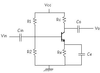
[Assume other required data]
mod(Av) = (hfe * RL')/(hie + (ðh * RL') )
Where ðh = ((hie * hoe) - (hfe * hre)) [Get hfe, hre, hie,hoe from data sheet]
ðh = 0.069
Hence
75 = (330 * Rc)/(4500 + (0.069 * Rc)
Hence
4.331 * Rc = 4500
Hence Rc = 1039.02 ohm
We use HSV for better gain
Hence Rc = 1.2 Kohm
Ic peak = Vo peak / RL'
Ic peak = 5.66/Rc = 4.714 mA
Icq = Ic peak + Ic min
Assume Ic min = 0
Hence Icq = 4.714 mA
Re = Vre/Icq
Hence Re = 1/(4.714 * (10 ^ -3)) = 318 ohm
Select lower std value of Re so that voltage drop across Re is less which increases the voltage swing of o/p
Hence Re = 270ohm
Select higher std val
Hence Vcc = 18V
s = (1 + hfe max)/(1 + ((hfe max * Re )/(Rb + Re))
Hence 10 = 1 + 450)/(1 + ((450 * 270)/(Rb + 270))
Hence Rb = 2485.1 V
Vr2 = Vbe + Vre = 07 + (4.714 * 0.27) = 1.87 V
Vr1 = Vcc - Vr2 = 16.02 V
Assume Vbe = 0.6V
R1/R2 = Vr1/Vr2 .............(A)
[Get R1 in terms of R2 & substitute in Rb]
Hence R1 = 8.124 * R2
Rb = R1 parallel R2 = (R1 * R2)/(R1 + R2) = (8.124 * R2)/9.124 = 0.89 * R2
Hence 2.485.1 = 0.89 * R2
Hence R2 = 2790.99 ohm
Select lower standard value to make circuit indepent of beta
Hence R2 = 2.7 K ohm
Substitute in (A) to find R1
R1 = 8.124 * 2700 = 21934.8 K ohm
Select higher standard value so that circuit draws minimum current
from supply
Hence R1 = 22 K ohm
Ce = 1/(2*pi * FL * Xce) = 235.78 µ F
Hence Ce = 270 µ F | 50 V
Xcb = ((Rb) parallel (hie))
Cb = 1/(2 * pi * FL * Xcb) = 4.06 µ F
Hence Cb = 4.2 µ F | 50 V
Xcc = Rc + RL [If RL[load resistance] is not specified thenassume amplifier is connected to a similar next stage. Hence RL = (Rb)parallel (hie)]
Cc = 1/(2 * pi * FL * Xcc) = 5.3 µ F
Hence Cc = 5.6 µ F | 50 V
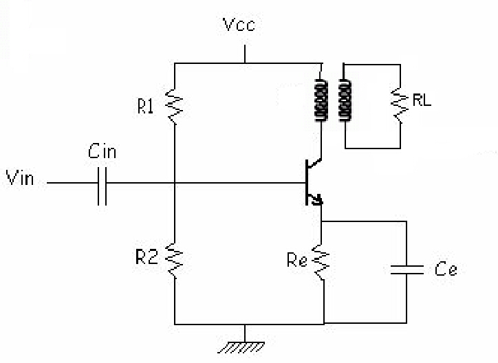
[Draw the figure with designed values. Do all this in 30 minutes (1.8
min per mark)]
1: Design for device
parameter variations
2: Design for midpoint biasing
3: Design for Zero thermal drift
4: Graphical methord
[Do not write text included in square bracket ]
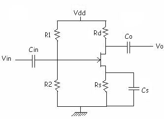
Vgs = Vp * (1 - sqrt(Id/Idss))
Vgs max = - 1.4 V, Vgs min = - 0.29 V,
Vgsq = (Vgs max + Vgs min)/2 = -0.845 V
Hence Rs = 620 ohm
Hence RL' = 2719 ohm
Assume RL = infinity
RL' = (rd) parallel (Rd)
Hence Rd = 2.87 K ohm
Select higher standard value
Hence Rd = 3.3 K ohm
Also
Vg = Vdd * R2/(R1 + R2)
Hence R1 = 0.47 * R2..................(A)
Assume R2 = 1 M ohm
Substitute in (A)
Hence R1 = 470 Kohm
Xcg = (R1) parallel (R2) = 319.72 ohm
Cg = 1/(2 * pi * FL * Xcg) = 0.0248 µ F
Select higher standard value
Hence Cg = 0.027 µ F | 25 V
Cd = 0.0248 µ F
Select higher standard value
Hence Cd = 0.027 µ F | 25 V
Select HSV
Hence Cs = 42 µ F | 25 V
[Draw the figure with designed values]
[Draw the figure]

Hence
Vgsq = Vp typ * (1 - sqrt(Idq/Idss typ)) = 0.75 V
Select HSV
Hence Rs = 220 ohm
Gain of JFET amplifier, mod(Av) = gm * RL'
RL is not given
Hence assume RL = infinity
RL' = (rd) parallel (Rd)
Rd = 3.03 Kohm
Select HSV
Hence Rd = 3.3 ohm
Hence Vdd = 20 V
Select HSV
Hence Cg = 0.018 µF | 50 V
Select HSV
Hence Cd = 0.01 µF | 50 V
Select HSV
Hence Cg = 81 µF | 50 V
[Draw the circuit with designed values]
We use self bias circuit
[Draw the figure]
Hence Vgsq = -1.87 V
Gain of JFET amplifier, mod(Av) = gm * RL'
RL is not given
assume RL = infinity
RL' = (rd) parallel (Rd)
Hence Rd = 8.33 Kohm
Select higher standard value
Hence Rd = 9.1 K ohm
Xcg = (Rg)
Cg = 1/(2 * pi * FL * Xcg) = 0.0079 µF
Select higher std value
Hence Cg = 0.01 µF | 25 V
Hence Cd = 0.0079 µF
Select higher std val
Hence Cd = 0.01 µF | 25 V
Select HSV
Hence Cg = 12 µF | 25 V
[Draw the circuit with designed values]
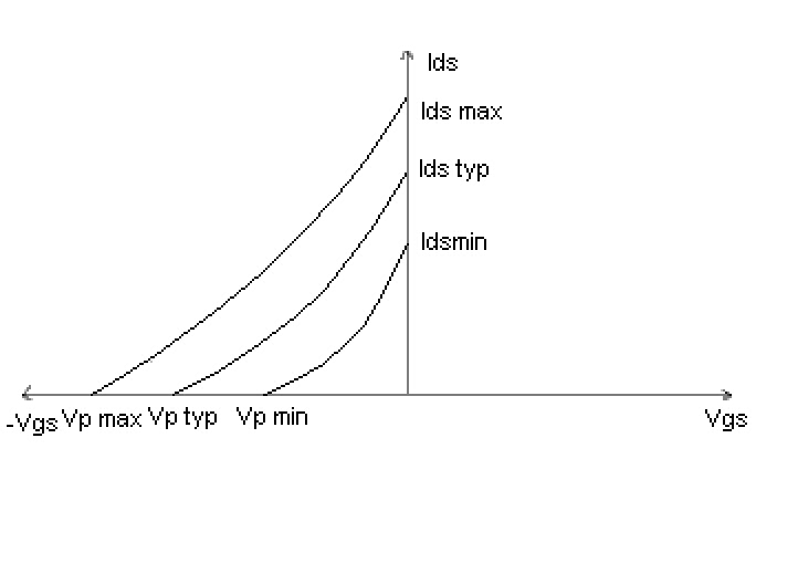
[In graphical methord draw the graph of Ids against Vds [Values given in data sheet.You will be given the value/s of or range of Ids (2 values(max or min) or range of values for device parameter variation & single value(typ) for other methods)]
[Plot the required value/s of Vgs & find Vgsq
& continue with the usual method. The answers in the 2 methods will
differ a lot for the same problem. For device parameter variation use max
& min curve to calculate Vgs max & min resp. For other methods
use typ curve unless mentioned otherwise ]
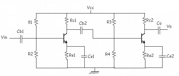
Av = Av1 * Av2
(Av1/Av2) = (Ro1/Ro2)
Assume (Ro1/R02) = 0.5
Hence Av2 = 2* Av1
Hence Av = 2 * ((Av1) ^ 2)
Hence 1000 = 2 * ((Av1) ^ 2)
Hence Av1 = 31.62
&Av2 = 63.24
We use BC 147A
63.24 = (220 * Rc2)/2700
Hence Rc2 = 776.18
Take higher std value
Hence Rc2 = 820 ohm
Hence Vceq2 = 4.617 ohm
Icq2 = Ic2peak + Ic2min
Assume Ic2min = 0
Ic2 peak = (Vopeak/Rc2) = 3.449 mA
Hence Icq2 = 3.449 mA
Hence Re2 = Vre2/Icq2
Hence Re2 = 289 ohm
Take LSV
Hence Re2 = 270 ohm
Hence Vcc = 10.445 V
Take Vcc = 12 V
Assume s = 8
Hence 8 = (1 + hfe)/(1 + ((hfe * Re2)/(Rb2 + Re2)))
[Substitute hfe, Re2 & find Rb2]
Hence Rb2 = 1971.13 ohm [Do not standardise]
VR4 = Vbe + (Icq2 * Re2)
Hence VR4 = 1.63 V
VR3 = Vcc - VR4
Hence VR3 = 10.368 V
(VR3/VR4) = (R3/R4)
Hence (R3/R4) = 6.356
Now Rb2 = 1971.13 = (R3 * R4)/(R3 + R4) = (6.356 * R4)/7.356
Hence R4 = Rb/0.864 = 2281.22 ohm
Take lower standard value
Hence R4 = 2.2 Kohm
Hence R3 = 6.642 * R4 = 13917.2 ohm
Select higher standard value
Hence R3 = 15 K ohm
Av1 = 2000/Av2 = 29.93
| Av1 | = (hfe typ * RL1)/hie
Hence RL1 = (Rc1) parallel (Zin2)
Where Zin2 = (R3) parallel (R4) parallel (hie) = 1121.6 ohm
Hence Rc1 = 546.21 ohm
Taking higher std value
Hence Rc1 = 560 ohm
Let Vceq1 = Vceq2 = 4.617 V
Vrc1 = Vrc2 = 2.828 V
Vre1 = Vre2 = 0.931 V
Icq1 = Vrc1/Rc1 = 5.05 mA
Re1 = Vre1/Icq1 = 184 ohm
R2 = R4 = 2.2 K ohm
Select higher standard value
Hence Ce1 = 120 µF
Taking higher standard value
Hence Ce2 = 62 µF
Cb1 = 1/(2 * pi * FL * Xcb1) = 1.418 µF
Taking higher std value
Hence Cb1 = 1.5 µF
Xcb2 = Rc1 + ((Rb2) parallel (hie))
Cb2 = 1/(2 * pi * FL * Xcb) = 4.261 µF
Taking higher std values
Hence Cb2 = 4.7 µF
Xco = Rc + RL
Co = 1/(2 * pi * FL * Xco) = 0.819 µF
Taking higher std value
HenceCo = 1 µF
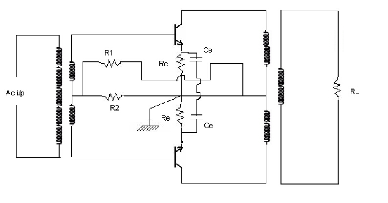
[Draw the figure with designed values. Do all this in about 36 - 40 minutes (1.8minper mark)]
Class A amplifier
Class B amplifier
Do not write text included in square bracket
Power transmitted to load, PL' = PL/nt = 5.555W
[nt = efficiency of transformer]
Assume nT = 90% or 0.9
Q = (Pq max)/(PL') = 2
Hence Pq max = 11.111 W
Select transistor with Pd > 2 * Pq max
Select ECN 149 with Pd max = 30 W
Vceq = Vcc - Vre = 10.8 V
Vce peak = Vceq - Vce sat = 9.8V
Ic peak = (2 * PL')/Vce peak = 1.134 A
Icq = Ic peak + Icmin
Assume Ic min = 0
Hence Icq = 1.134 A
Pre = sqr(Vre)/Re = 1.44 W
Select Re = 1 ohm | 3 W
Ce = 1/(2 * pi * FL * RL) = 7957.74 µF
Since Ce is very high we leave Re unbypassed
s = (1 + hfe max)/(1 + ((hfe max * Re )/(Rb + Re))
We have Rb = 9.89 ohm
Vr2 = Vbe + (Icq * Re) = 1.834 ohm
Vr1 = Vcc - Vr2 = 10.166 ohm
R1/R2 = Vr1/Vr2 = 5.543
Hence R1 = 5.543 * R2 .............(A)
Rb = R1 parallel R2 = (R1 * R2)/(R1 + R2) = (5.543 * R2)/6.543
Hence R2 = 11.67 ohm
Select lower standard value to make circuit indepent of beta
PR2 = ((VR2) ^ 2)/R2 = 0.336 W
Hence R2 = 10 ohm | 0.75 W
Substituting in (A) we get
R1 = 55.43 ohm
Select higher std value
Hence R1 = 56 ohm
PR1 = ((VR1) ^ 2)/R1 = 1.86 W
Select R1 = 56 ohm | 3.75 W
RL' = (sqr(N1/N2)) * RL
Hence (N1/N2) = 1.697
Select audio frequency transformer with turns ratio 1: 1.697
PL' FL = (Vce peak * Ic peak)/2 = 5.556 W
Pi dc = (Vcc * Icq) + (Vcc ^ 2)/(R1 + R2) = 15.79 W
Hence n FL = 0.3518 or 35.18 %
For a class A amp max power dissipation occurs under no signal condition
Hence PD no signal = 30 W
Q = (Pq max)/PL') = 1/5
PL = (I^2)/RL = 49/3 = 16.33W
PL' =PL/nT = 18.148 W
Hence Pqmax = 3.629 W
Select transistor with Pd > 2 * Pq max
Select transistor ECN 149 with Pdmax = 30W
Vre = Vcc/10
Hence Vre = 2.5 V
Vceq = Vcc - Vre = 25 - 2.5
Hence Vceq = 22.5 V
Vce peak = Vceq - Vce sat = 21.5 V
Ic peak = (2 * PL')/Vce peak = 2.519 A
Assume Ic min = 0
Icq = Icpeak + Icmin = 2.519A
Idc full wave = (2 * Idc peak)/pi = 0.967 A
Idc half wave = Idc peak/pi = 0.483 A
Pre = sqr(Vre)/Re = 1.225 W
Select Re = 5.1 ohm |3W
Ce = 1/(2 * pi * FL * RL)
Ce is too high hence leave Re unbypassed
s = (1 + hfe max)/(1 + ((hfe max * Re )/(Rb + Re))
Rb = 50.44 ohm [Show the calculations]
Vr2 = Vbe + (Idc half wave * Re) = 3.163 V
Vr1 = Vcc - Vr2 = 21.83 V
Assume Vbe = 0.6V
R1/R2 = Vr1/Vr2 = 6.903 .............(A)
Rb = R1 parallel R2 = (R1 * R2)/(R1 + R2)
Hence R2 = 57.747 ohm = 56 (LSV)
PR2 = (Vr1 ^ 2)/R1 = 0.178 W
Select lower standard value to make circuit indepent of beta
Hence R2 = 56 ohm | 0.5 W
Substitute in (A) to find R1 R1 = 386.56 ohm
PR1 = 1.22 W
Select higher standard value so that circuit draws minimum current from
supply
Hence R1 = 390 ohm| 3 W
RL' = (sqr(N1/N2)) * RL
Hence (N1/N2) = 2.172
Hence N1:N2 = 2.172 : 1
Power rating of primary > PL'
ie power rating of primary > 18.148 ohm
Select audio frequency transformer with turns ratio 1:(N1/N2)
Select centre tap transformer with turns ratio 2.172 : 2.172 : 1 &
power rating of 25 W
[Draw the circuit diagram with calculated values]